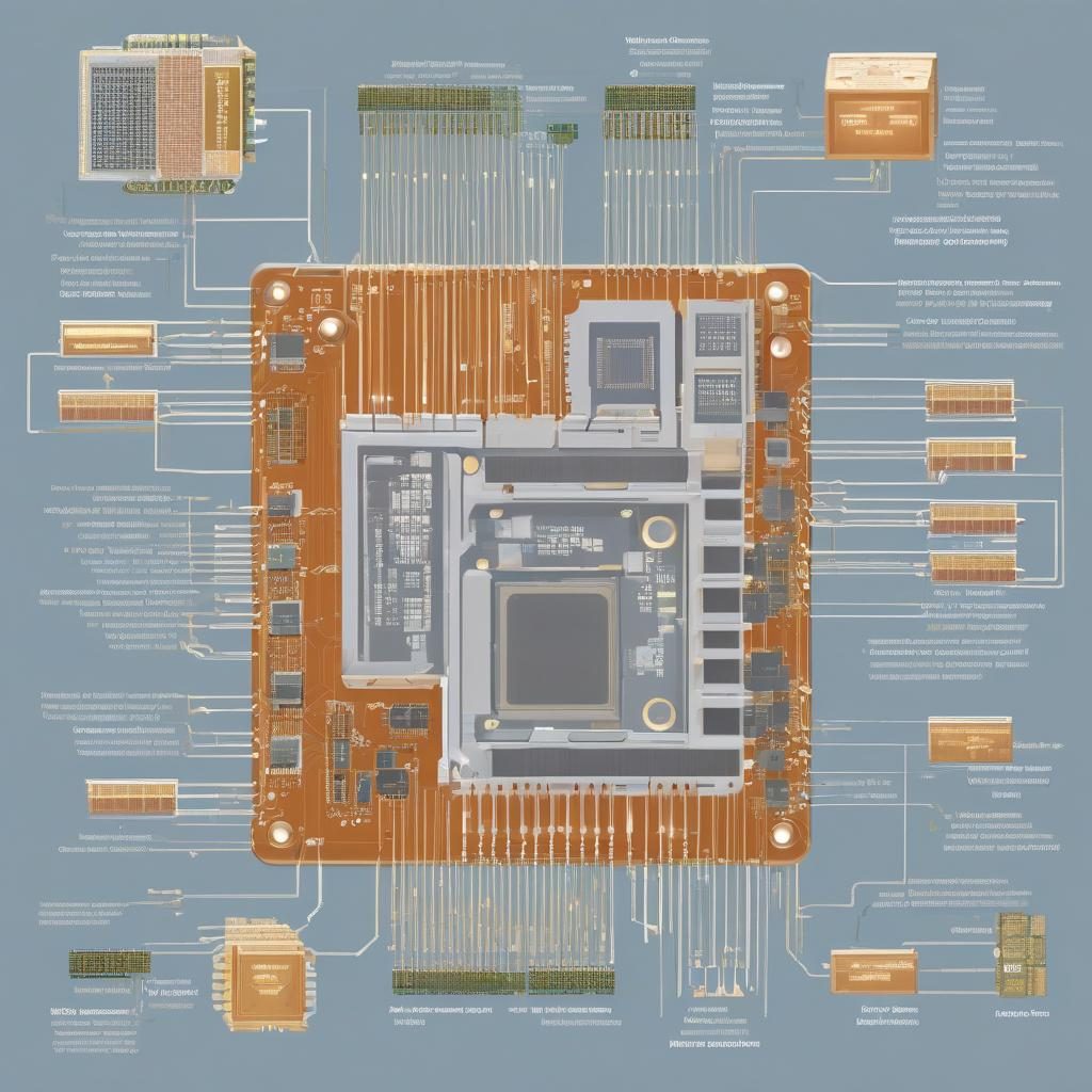
EDA Solutions
In the context of semiconductor design, "EDA solutions verification" refers to the use of Electronic Design Automation (EDA) tools to thoroughly test and validate a semiconductor chip design, ensuring it functions as intended and meets all performance requirements before moving to manufacturing, by simulating various scenarios and identifying potential issues within the circuit layout and functionality

IP Solutions
In electronic design, a semiconductor intellectual property core (SIP core), IP core or IP block is a reusable unit of logic, cell, or integrated circuit layout design that is the intellectual property of one party. IP cores can be licensed to another party or owned and used by a single party. The term comes from the licensing of the patent or source code copyright that exists in the design. Designers of system on chip (SoC), application-specific integrated circuits (ASIC) and systems of field-programmable gate array (FPGA) logic can use IP cores as building blocks.

System On Modules
A "System on Module for FPGA" (SOM) is a small, pre-built circuit board that integrates a Field Programmable Gate Array (FPGA) with other necessary components like memory, power management circuitry, and various interface controllers, allowing developers to quickly incorporate custom FPGA logic into their systems without designing the entire hardware from scratch; essentially offering a ready-to-use building block for embedded applications that require high flexibility and custom logic capabilities

Silicon Reliability Qualification
Silicon reliability testing is a process that evaluates the durability and quality of semiconductors, ensuring they perform well in harsh conditions. This testing is important in industries like aerospace, automotive, and telecommunications, where safety and performance are critical.

©Copyright. All rights reserved.
We need your consent to load the translations
We use a third-party service to translate the website content that may collect data about your activity. Please review the details in the privacy policy and accept the service to view the translations.